Journals > > Topics > Optical Devices
Optical Devices|965 Article(s)
Simulation and Experimental Analysis of Aspherical Combined Liquid Lens Based on Flat Electrode
Meimei Kong, Yuan Dong, Chunsheng Xu, Yue Liu, Yinyan Xue, Mingyang Li, and Shuhan Zhang
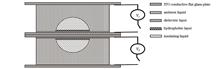
ObjectiveAs an important branch of microfluidic optics, microfluidic optics has become a key technology to promote the development of highly miniaturized and functional optics. Liquid lenses are a common form of microfluidic optical lenses, and as an important part of optical systems, they have obvious advantages over solid lenses, such as a reconfigurable geometry and tunable refractive index. At present, researchers have explored various techniques and tuning mechanisms to make liquid lenses, including fluid pressure lenses, electromagnetic wave lenses, electrowetting lenses and dielectrophoresis lenses. Unlike electrowetting driven liquid lenses, dielectrophoresis driven liquid lenses do not require conducting liquid and do not produce problems such as evaporation or microbubbles. To correct aberrations in practical applications, it is necessary to design a liquid lens with an aspherical surface, which has the advantages of a simple structure and easy realization because of the use of continuous electrodes compared with patterned electrodes.MethodsBased on the dielectrophoresis effect, we design an aspherical combined liquid lens based on flat electrode. A certain dielectric constant difference exists between the two liquid materials filled with miscible pairs in the cavity. When the external voltage is applied, the droplet with high dielectric constant will move along the electric field direction and squeeze the droplet with low dielectric constant, and the curvature radius of the liquid-liquid interface will change. By adjusting the voltage applied to the two indium tin oxide (ITO) conductive glass flats in the middle, the curvature radius of the liquid-liquid interface can be changed to adjust the focal length. First, a model of an aspherical combined liquid lens based on a parallel flat electrode under different voltages is built by COMSOL, and the surface profile data of the aspherical interface are obtained. Then, the aspherical surface profile data and aspherical formula are fitted by MATLAB to obtain the corresponding aspherical coefficient. Finally, on this basis, the optical model of the aspherical combined liquid lens based on flat electrode is built by Zemax, and the focal length of the aspherical combined liquid lens under different voltages is obtained.Results and DiscussionsFirst, we compare the aspherical combined liquid lens based on the flat electrode with the aspherical single liquid lens, which has the same liquid material and droplet volume as the aspherical composite liquid lens. The results show that the aspherical combined liquid lens has a smaller focal length and stronger focusing ability than the aspherical single liquid lens and is more suitable for camera lenses requiring a large depth of field (Fig. 5). In order to further study the characteristics of aspherical combined liquid lens based on flat electrode, COMSOL software is used to simulate the change of the interface profile of aspherical combined liquid lens based on flat electrode under different parallelism. In the simulation process of the model, the lower flat is set to be placed horizontally. When the upper and lower flat are not parallel, that is, the upper flat and the horizontal direction have a certain tilt angle, the electric field distribution in the liquid lens model is analyzed (Fig. 6). The interface profile data obtained in COMSOL is derived, then MATLAB is applied to fit the profile, and the comparison and analysis of aspherical combined liquid lenses with different parallelism is carried out by using Zemax. It is found that the focal length of the aspherical combined liquid lens is little affected when the flat electrode has a small inclination (1° to 4°) (Fig. 7).ConclusionsBased on the dielectrophoresis effect, an aspherical combined liquid lens based on flat electrode is designed in this study. The liquid lens consists of four ITO conductive flat glass plates, cavities, dielectric layers and hydrophobic layers parallel up and down. The focal length of the aspherical combined liquid lens under different voltages is calculated by using the relevant optical model, and the results show that the focal length of the aspherical combined liquid lens is smaller than that of the aspherical single liquid lens, and the imaging quality is better. The influence of the parallelism of the flat electrode on the focal length of the aspherical combined liquid lens is also discussed. The aspherical combined liquid lens is prepared experimentally, and its focal length and imaging resolution are measured. When the operating voltage increases from 0 to 280 V, the focal length varies from 28.7135 mm to 20.1943 mm, which is basically consistent with the simulation. The feasibility of the lens structure is verified by experiments. The imaging resolution is up to 49.8244 lp/mm. The designed aspherical combined liquid lens based on a flat electrode can provide a new scheme for the high-quality imaging of liquid lenses and their applications and can expand the application. ObjectiveAs an important branch of microfluidic optics, microfluidic optics has become a key technology to promote the development of highly miniaturized and functional optics. Liquid lenses are a common form of microfluidic optical lenses, and as an important part of optical systems, they have obvious advantages over solid lenses, such as a reconfigurable geometry and tunable refractive index. At present, researchers have explored various techniques and tuning mechanisms to make liquid lenses, including fluid pressure lenses, electromagnetic wave lenses, electrowetting lenses and dielectrophoresis lenses. Unlike electrowetting driven liquid lenses, dielectrophoresis driven liquid lenses do not require conducting liquid and do not produce problems such as evaporation or microbubbles. To correct aberrations in practical applications, it is necessary to design a liquid lens with an aspherical surface, which has the advantages of a simple structure and easy realization because of the use of continuous electrodes compared with patterned electrodes.MethodsBased on the dielectrophoresis effect, we design an aspherical combined liquid lens based on flat electrode. A certain dielectric constant difference exists between the two liquid materials filled with miscible pairs in the cavity. When the external voltage is applied, the droplet with high dielectric constant will move along the electric field direction and squeeze the droplet with low dielectric constant, and the curvature radius of the liquid-liquid interface will change. By adjusting the voltage applied to the two indium tin oxide (ITO) conductive glass flats in the middle, the curvature radius of the liquid-liquid interface can be changed to adjust the focal length. First, a model of an aspherical combined liquid lens based on a parallel flat electrode under different voltages is built by COMSOL, and the surface profile data of the aspherical interface are obtained. Then, the aspherical surface profile data and aspherical formula are fitted by MATLAB to obtain the corresponding aspherical coefficient. Finally, on this basis, the optical model of the aspherical combined liquid lens based on flat electrode is built by Zemax, and the focal length of the aspherical combined liquid lens under different voltages is obtained.Results and DiscussionsFirst, we compare the aspherical combined liquid lens based on the flat electrode with the aspherical single liquid lens, which has the same liquid material and droplet volume as the aspherical composite liquid lens. The results show that the aspherical combined liquid lens has a smaller focal length and stronger focusing ability than the aspherical single liquid lens and is more suitable for camera lenses requiring a large depth of field (Fig. 5). In order to further study the characteristics of aspherical combined liquid lens based on flat electrode, COMSOL software is used to simulate the change of the interface profile of aspherical combined liquid lens based on flat electrode under different parallelism. In the simulation process of the model, the lower flat is set to be placed horizontally. When the upper and lower flat are not parallel, that is, the upper flat and the horizontal direction have a certain tilt angle, the electric field distribution in the liquid lens model is analyzed (Fig. 6). The interface profile data obtained in COMSOL is derived, then MATLAB is applied to fit the profile, and the comparison and analysis of aspherical combined liquid lenses with different parallelism is carried out by using Zemax. It is found that the focal length of the aspherical combined liquid lens is little affected when the flat electrode has a small inclination (1° to 4°) (Fig. 7).ConclusionsBased on the dielectrophoresis effect, an aspherical combined liquid lens based on flat electrode is designed in this study. The liquid lens consists of four ITO conductive flat glass plates, cavities, dielectric layers and hydrophobic layers parallel up and down. The focal length of the aspherical combined liquid lens under different voltages is calculated by using the relevant optical model, and the results show that the focal length of the aspherical combined liquid lens is smaller than that of the aspherical single liquid lens, and the imaging quality is better. The influence of the parallelism of the flat electrode on the focal length of the aspherical combined liquid lens is also discussed. The aspherical combined liquid lens is prepared experimentally, and its focal length and imaging resolution are measured. When the operating voltage increases from 0 to 280 V, the focal length varies from 28.7135 mm to 20.1943 mm, which is basically consistent with the simulation. The feasibility of the lens structure is verified by experiments. The imaging resolution is up to 49.8244 lp/mm. The designed aspherical combined liquid lens based on a flat electrode can provide a new scheme for the high-quality imaging of liquid lenses and their applications and can expand the application.
Acta Optica Sinica
- Publication Date: Apr. 25, 2024
- Vol. 44, Issue 8, 0823002 (2024)

Terahertz Multidimensional-Multiplexing and Refractive-Index-Sensing Integrated Device
Lu Jie, Haisu Li, Yajing Liu, Jianshuai Wang, Guobin Ren, and Li Pei
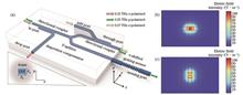
ObjectiveTerahertz waves featuring broad bandwidths play an increasingly important role in next-generation communication systems. For both terahertz wired and wireless communications, terahertz waveguide integrated devices providing“on-line”signal processing functionalities are in vital demand. In the next-generation communication system, the multiplexing technology around the electromagnetic wave physical parameters such as terahertz radiation polarization, frequency, and phase is an effective solution to enhancing spectrum efficiency. Additionally, the future Internet of Everything information system should have a real-time monitoring function of communication environmental parameters (temperature, humidity, etc.). Given the above technical requirements of multidimensional multiplexing and environmental sensing, novel terahertz functional integrated devices for high-speed information transmission-manipulation-perception fusion should be studied urgently. Several terahertz silicon-based waveguide devices have been demonstrated, but the planar structure restricts the spatial degree of freedom for the devices, which means the devices can only be integrated in a 2D plane. Terahertz fiber-based devices are substrate-free to provide terahertz wave routing abilities along any spatial direction. Nevertheless, most of the reported terahertz fiber devices offer a single functionality, remaining a significant scope of multiple device integration. Thus, we propose a polarization-maintaining subwavelength fiber-based multidimensional multiplexing and sensing integrated device which is composed of fiber bends, a 50/50 Y-splitter, directional couplers, and Bragg gratings. The proposed fiber device provides (de)multiplexing in an additional direction that is orthogonal to the 2D space in contrast to the planar devices. Meanwhile, the device integrates multiple functionalities, including frequency- and polarization-(de)multiplexing, dispersion compensation, and surrounding refractive index sensing. In a nutshell, the integrated device provides exciting perspectives for boosting transmission capacity and developing communication-sensing integration of the next-generation communication systems.MethodsThe finite element analysis method and finite-difference time-domain model are employed in our study. First, the finite element analysis method is adopted to calculate the transmission parameters (fractional power in the core, loss, group velocity dispersion, etc.) of terahertz subwavelength fibers with different cross-sectional parameters to design polarization-maintaining fibers supporting low-loss and low-dispersion transmission. Then, S-shaped and 90° bending fibers are designed using Bessel curves. Furthermore, the finite-difference time-domain model is utilized to analyze the transmission characteristics of S-shaped and 90° bending fibers. Then, two S-shaped bending fibers with the same bending radius are utilized to form a Y-splitter. In the next step, we leverage the supermode theory as a theoretical guide and the finite element analysis method as a tool to calculate the required coupling length of the directional couplers. Additionally, the finite element analysis method is employed to investigate the effects of grating cell cross-section parameters, thickness, and number of cycles on grating performance (e.g., transmission and dispersion compensation), and thus accomplish the structural design of uniform gratings. Finally, the performance of the proposed terahertz devices including directional couplers, Y-splitter, uniform grating, and phase-shifted grating is simulated and analyzed using the time-domain finite difference method.Results and DiscussionsWe present terahertz subwavelength rectangular fibers, bending fibers, Y-splitter, directional couplers, uniform grating, phase-shift grating, and multidimensional-multiplexing and refractive-index-sensing integrated devices. First, the subwavelength fiber supports low-loss (below 0.051 dB/mm) and high-birefringent (beyond 0.03) transmissions at a target bandwidth over 0.24-0.28 THz as shown in Fig. 2. Second, the transmission of S-shaped bending fibers with a bending radius of 10 mm is slightly higher than that of 90° bending fibers in the frequency range of 0.24-0.28 THz, whose transmission is higher than -1 dB at the operating frequency of 0.25 THz [Fig. 4(d)]. Thanks to the high transmission of x-bent S-shaped bends, a 50/50 Y-splitter can be readily designed using two bends with the same radius of 10 mm. Third, for the x-placed x-bent directional coupler, high transmission (above -3 dB) and high ER (above 7 dB) are obtained for both x-polarization and y-polarization modes when coupling lengths are in the range of 11.8-12.3 mm. Finally, the integrated device achieves simultaneously polarization and frequency (de)multiplexing, with high transmissions [drop port: -5.94 dB for 0.25 THz x-polarization with dispersion compensation; through port: -7.20 dB for 0.25 THz y-polarization, -2.02 dB for 0.27 THz x-polarization] and high ER (drop port: 15.16 dB; through port: 8.06 dB). Additionally, the device integrates fiber Bragg gratings, allowing both zero-GVD dispersion compensation and refractive-index sensing (sensitivity of 0.181 THz/RIU) abilities (Figs. 17 and 18).ConclusionsWe propose and analyze a terahertz multidimensional-multiplexing and sensing integrated device based on subwavelength birefringent fibers, composed of fiber bends, 50/50 Y-splitter, directional couplers, and Bragg gratings. First, a directional coupler with high transmission and high extinction ratio is designed by introducing a bent fiber to achieve polarization and frequency (de)multiplexing functions. Second, the uniform grating and phase-shift grating in the integrated device enable dispersion compensation and environmental refractive index sensing respectively. Terahertz subwavelength fiber devices feature dense integration in 3D space and efficient transmission, which provides novel design solutions for the integrated terahertz wave transmission-manipulation-sensing information system. Meanwhile, we also envision that many more components such as modulators and imaging devices will be further integrated on the terahertz fiber platform. ObjectiveTerahertz waves featuring broad bandwidths play an increasingly important role in next-generation communication systems. For both terahertz wired and wireless communications, terahertz waveguide integrated devices providing“on-line”signal processing functionalities are in vital demand. In the next-generation communication system, the multiplexing technology around the electromagnetic wave physical parameters such as terahertz radiation polarization, frequency, and phase is an effective solution to enhancing spectrum efficiency. Additionally, the future Internet of Everything information system should have a real-time monitoring function of communication environmental parameters (temperature, humidity, etc.). Given the above technical requirements of multidimensional multiplexing and environmental sensing, novel terahertz functional integrated devices for high-speed information transmission-manipulation-perception fusion should be studied urgently. Several terahertz silicon-based waveguide devices have been demonstrated, but the planar structure restricts the spatial degree of freedom for the devices, which means the devices can only be integrated in a 2D plane. Terahertz fiber-based devices are substrate-free to provide terahertz wave routing abilities along any spatial direction. Nevertheless, most of the reported terahertz fiber devices offer a single functionality, remaining a significant scope of multiple device integration. Thus, we propose a polarization-maintaining subwavelength fiber-based multidimensional multiplexing and sensing integrated device which is composed of fiber bends, a 50/50 Y-splitter, directional couplers, and Bragg gratings. The proposed fiber device provides (de)multiplexing in an additional direction that is orthogonal to the 2D space in contrast to the planar devices. Meanwhile, the device integrates multiple functionalities, including frequency- and polarization-(de)multiplexing, dispersion compensation, and surrounding refractive index sensing. In a nutshell, the integrated device provides exciting perspectives for boosting transmission capacity and developing communication-sensing integration of the next-generation communication systems.MethodsThe finite element analysis method and finite-difference time-domain model are employed in our study. First, the finite element analysis method is adopted to calculate the transmission parameters (fractional power in the core, loss, group velocity dispersion, etc.) of terahertz subwavelength fibers with different cross-sectional parameters to design polarization-maintaining fibers supporting low-loss and low-dispersion transmission. Then, S-shaped and 90° bending fibers are designed using Bessel curves. Furthermore, the finite-difference time-domain model is utilized to analyze the transmission characteristics of S-shaped and 90° bending fibers. Then, two S-shaped bending fibers with the same bending radius are utilized to form a Y-splitter. In the next step, we leverage the supermode theory as a theoretical guide and the finite element analysis method as a tool to calculate the required coupling length of the directional couplers. Additionally, the finite element analysis method is employed to investigate the effects of grating cell cross-section parameters, thickness, and number of cycles on grating performance (e.g., transmission and dispersion compensation), and thus accomplish the structural design of uniform gratings. Finally, the performance of the proposed terahertz devices including directional couplers, Y-splitter, uniform grating, and phase-shifted grating is simulated and analyzed using the time-domain finite difference method.Results and DiscussionsWe present terahertz subwavelength rectangular fibers, bending fibers, Y-splitter, directional couplers, uniform grating, phase-shift grating, and multidimensional-multiplexing and refractive-index-sensing integrated devices. First, the subwavelength fiber supports low-loss (below 0.051 dB/mm) and high-birefringent (beyond 0.03) transmissions at a target bandwidth over 0.24-0.28 THz as shown in Fig. 2. Second, the transmission of S-shaped bending fibers with a bending radius of 10 mm is slightly higher than that of 90° bending fibers in the frequency range of 0.24-0.28 THz, whose transmission is higher than -1 dB at the operating frequency of 0.25 THz [Fig. 4(d)]. Thanks to the high transmission of x-bent S-shaped bends, a 50/50 Y-splitter can be readily designed using two bends with the same radius of 10 mm. Third, for the x-placed x-bent directional coupler, high transmission (above -3 dB) and high ER (above 7 dB) are obtained for both x-polarization and y-polarization modes when coupling lengths are in the range of 11.8-12.3 mm. Finally, the integrated device achieves simultaneously polarization and frequency (de)multiplexing, with high transmissions [drop port: -5.94 dB for 0.25 THz x-polarization with dispersion compensation; through port: -7.20 dB for 0.25 THz y-polarization, -2.02 dB for 0.27 THz x-polarization] and high ER (drop port: 15.16 dB; through port: 8.06 dB). Additionally, the device integrates fiber Bragg gratings, allowing both zero-GVD dispersion compensation and refractive-index sensing (sensitivity of 0.181 THz/RIU) abilities (Figs. 17 and 18).ConclusionsWe propose and analyze a terahertz multidimensional-multiplexing and sensing integrated device based on subwavelength birefringent fibers, composed of fiber bends, 50/50 Y-splitter, directional couplers, and Bragg gratings. First, a directional coupler with high transmission and high extinction ratio is designed by introducing a bent fiber to achieve polarization and frequency (de)multiplexing functions. Second, the uniform grating and phase-shift grating in the integrated device enable dispersion compensation and environmental refractive index sensing respectively. Terahertz subwavelength fiber devices feature dense integration in 3D space and efficient transmission, which provides novel design solutions for the integrated terahertz wave transmission-manipulation-sensing information system. Meanwhile, we also envision that many more components such as modulators and imaging devices will be further integrated on the terahertz fiber platform.
Acta Optica Sinica
- Publication Date: Apr. 25, 2024
- Vol. 44, Issue 8, 0823001 (2024)
Design of Three-Core Structure Broadband Coupler Based on Hollow-Core Anti-Resonant Optical Fiber
Le Chen, and Mingyang Chen
ObjectiveThe special wavelength position of terahertz waves makes them the link between microphotonics and macroscopic electronics. However, the terahertz wave transmission in free space is easily affected by the water vapor absorption in the air. The optical fiber structure is proposed to transmit terahertz waves and realize effective transmission control. Among them, the hollow-core THz fiber based on the anti-resonant principle can limit the wave transmission in the air fiber core, which greatly reduces the influence of material absorption. The optical fiber coupler is the key device for beam splitting and transmission tailoring. Due to the existence of absorption loss in THz fiber, the insertion losses of THz fiber couplers are usually large and affect their utilization. Although the transmission loss of THz fibers with hollow-core structures is low, the design of THz couplers with broadband beam splitting is generally difficult.MethodsWe propose a hollow-core anti-resonant fiber coupler based on the three-core symmetry structure. By employing its structure symmetry, broadband beam splitting can be realized, and the transmission loss of the coupler can be reduced via the hollow-core structure. The mode and coupling characteristics of the coupler are analyzed by the finite element method, and the relationship between the coupling length and the fiber structure parameters is verified. The mode loss characteristics of the coupler are analyzed, and then the beam splitting structure with low loss and wide bandwidth is obtained.Results and DiscussionsWe design a hollow-core three-core anti-resonant fiber. At the frequency of 1 THz, the coupling length increases with the rising core distance (Fig. 4). As can be seen from the relation curve between D1 and binding loss, since the even mode field expands more to the intermediate core, the increase in D1 leads to the growing mode field, and the improvement in the binding ability of the core reduces the binding loss, while the odd mode is less affected by D1 [Fig. 5(a)]. With the increasing D1, the total loss of even mode obviously shows a downward trend, while the change of odd mode is not obvious. Compared with the mode loss of single-core fiber, the total odd-mode loss of the three-core structure is always smaller than that of the single-core structure in the shown interval. Therefore, using the three-core structure can actually obtain smaller mode losses. This is also consistent with the theory that the larger core size leads to lower mode losses [Fig. 5(c)]. The coupling length decreases slowly with the rising dr when the separation hole spacing d is small. As dr spacing increases, the coupling length decreases linearly (Fig. 6). Since the odd-mode field extends more to the intermediate core, the dr increase is easier to increase its mode field, thereby reducing the mode binding loss, while the even-mode field is relatively independent of each core, and thus the change of dr has little effect on it [Fig. 7(a)]. With the increasing dr, the absorption loss shows an obvious downward trend, and the total mode loss is mainly determined by the absorption loss [Fig. 7(b)]. With the rising spacing dr, the total loss of odd mode shows an obvious downward trend, while that of even mode mainly decreases under small dr values, and the further increase in dr value has little influence on it [Fig. 7(c)]. The relationship between the output optical power under the influence of mode transmission loss and transmission distance and coupling length is shown in Eq. (6) and Fig. 8. In all bandwidth ranges, the polarization-related loss is lower than 0.2 dB. The two polarization curves indicate that the coupler is not sensitive to polarization, the insertion loss is less than 3.5 dB in the range of 0.82-1.34 THz, and the bandwidth can reach 0.52 THz. This coupler is found to feature wide bandwidth and low loss transmission (Fig. 9). Transmission loss has less effect on the loss of the device (Fig. 10). The two-core coupler is in the range of 0.9-1.1 THz, the insertion loss is less than 3.45 dB, and the bandwidth is 0.2 THz. In the working bandwidth range, the two output ports cannot output the same power, and when the output power difference between the two ports is less than 0.1 dB, the corresponding bandwidth is 1 THz, with a large output power difference. The working bandwidth of the three-core structure coupler and the two-core structure coupler is relatively narrow (Fig. 12).ConclusionsWe design an anti-resonant air-core three-core terahertz fiber coupler with cycloolefin copolymer as the base material. The mode analysis and calculation of the new structure of the terahertz waveguide are carried out by COMSOL multi-physics simulation coupling software, and the mode field distribution among waveguides and the mode coupling characteristics between fiber cores are analyzed. Finite element analysis and full vector beam propagation method are employed to analyze the structural parameters, coupling length and loss effects, bandwidth, and other characteristics. The results show that the coupling length increases with the rising core spacing and decreases with the growing hole spacing, and the mode transmission loss has little effect on the insertion loss of the device. Due to the symmetry, the three-core structure can realize the uniform beam splitting of 1×2 light, the working bandwidth reaches 0.52 THz, and the insertion loss is less than 3.5 dB, with the polarization-related loss less than 0.2 dB. ObjectiveThe special wavelength position of terahertz waves makes them the link between microphotonics and macroscopic electronics. However, the terahertz wave transmission in free space is easily affected by the water vapor absorption in the air. The optical fiber structure is proposed to transmit terahertz waves and realize effective transmission control. Among them, the hollow-core THz fiber based on the anti-resonant principle can limit the wave transmission in the air fiber core, which greatly reduces the influence of material absorption. The optical fiber coupler is the key device for beam splitting and transmission tailoring. Due to the existence of absorption loss in THz fiber, the insertion losses of THz fiber couplers are usually large and affect their utilization. Although the transmission loss of THz fibers with hollow-core structures is low, the design of THz couplers with broadband beam splitting is generally difficult.MethodsWe propose a hollow-core anti-resonant fiber coupler based on the three-core symmetry structure. By employing its structure symmetry, broadband beam splitting can be realized, and the transmission loss of the coupler can be reduced via the hollow-core structure. The mode and coupling characteristics of the coupler are analyzed by the finite element method, and the relationship between the coupling length and the fiber structure parameters is verified. The mode loss characteristics of the coupler are analyzed, and then the beam splitting structure with low loss and wide bandwidth is obtained.Results and DiscussionsWe design a hollow-core three-core anti-resonant fiber. At the frequency of 1 THz, the coupling length increases with the rising core distance (Fig. 4). As can be seen from the relation curve between D1 and binding loss, since the even mode field expands more to the intermediate core, the increase in D1 leads to the growing mode field, and the improvement in the binding ability of the core reduces the binding loss, while the odd mode is less affected by D1 [Fig. 5(a)]. With the increasing D1, the total loss of even mode obviously shows a downward trend, while the change of odd mode is not obvious. Compared with the mode loss of single-core fiber, the total odd-mode loss of the three-core structure is always smaller than that of the single-core structure in the shown interval. Therefore, using the three-core structure can actually obtain smaller mode losses. This is also consistent with the theory that the larger core size leads to lower mode losses [Fig. 5(c)]. The coupling length decreases slowly with the rising dr when the separation hole spacing d is small. As dr spacing increases, the coupling length decreases linearly (Fig. 6). Since the odd-mode field extends more to the intermediate core, the dr increase is easier to increase its mode field, thereby reducing the mode binding loss, while the even-mode field is relatively independent of each core, and thus the change of dr has little effect on it [Fig. 7(a)]. With the increasing dr, the absorption loss shows an obvious downward trend, and the total mode loss is mainly determined by the absorption loss [Fig. 7(b)]. With the rising spacing dr, the total loss of odd mode shows an obvious downward trend, while that of even mode mainly decreases under small dr values, and the further increase in dr value has little influence on it [Fig. 7(c)]. The relationship between the output optical power under the influence of mode transmission loss and transmission distance and coupling length is shown in Eq. (6) and Fig. 8. In all bandwidth ranges, the polarization-related loss is lower than 0.2 dB. The two polarization curves indicate that the coupler is not sensitive to polarization, the insertion loss is less than 3.5 dB in the range of 0.82-1.34 THz, and the bandwidth can reach 0.52 THz. This coupler is found to feature wide bandwidth and low loss transmission (Fig. 9). Transmission loss has less effect on the loss of the device (Fig. 10). The two-core coupler is in the range of 0.9-1.1 THz, the insertion loss is less than 3.45 dB, and the bandwidth is 0.2 THz. In the working bandwidth range, the two output ports cannot output the same power, and when the output power difference between the two ports is less than 0.1 dB, the corresponding bandwidth is 1 THz, with a large output power difference. The working bandwidth of the three-core structure coupler and the two-core structure coupler is relatively narrow (Fig. 12).ConclusionsWe design an anti-resonant air-core three-core terahertz fiber coupler with cycloolefin copolymer as the base material. The mode analysis and calculation of the new structure of the terahertz waveguide are carried out by COMSOL multi-physics simulation coupling software, and the mode field distribution among waveguides and the mode coupling characteristics between fiber cores are analyzed. Finite element analysis and full vector beam propagation method are employed to analyze the structural parameters, coupling length and loss effects, bandwidth, and other characteristics. The results show that the coupling length increases with the rising core spacing and decreases with the growing hole spacing, and the mode transmission loss has little effect on the insertion loss of the device. Due to the symmetry, the three-core structure can realize the uniform beam splitting of 1×2 light, the working bandwidth reaches 0.52 THz, and the insertion loss is less than 3.5 dB, with the polarization-related loss less than 0.2 dB.
Acta Optica Sinica
- Publication Date: Apr. 10, 2024
- Vol. 44, Issue 7, 0723003 (2024)
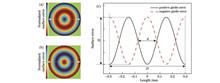
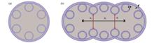
Method of Measuring Surface Error Peak to Valley of Micro Lens Based on Far-Field Light Distribution
Le Tang, Liangping Xia, Man Zhang, Weiguo Zhang, Hao Sun, Chunyan Wang, Suihu Dang, and Chunlei Du
ObjectiveIn the field of optics, the miniaturization and integration of optical systems and optical chips are inevitable trends. Micro lenses, as core devices, are widely used in optical imaging, homogenizing lighting, and optical communication. The accuracy of the surface shape determines the optical properties of micro lenses, making the detection of surface shape errors crucial. During fabrication, the nonlinear effect of photoresist often leads to the appearance of convex or concave annular errors on the micro lens surface. These annular errors significantly impact the optical performance of micro lenses, necessitating the development of a method to quickly detect them. Compared with the traditional profiler, Hartmann wavefront detection, and interferometry methods, this method ensures a simpler test light path, easier operation, and improved test efficiency.MethodsThe study focused on the impact of surface shape errors on the distribution of light fields, based on the structure model of the banded error. The position of the boundary (R1) of the light spot formed by different banded errors was calculated following the principles of geometrical optics. Additionally, a method was proposed to determine the surface shape error of the band by analyzing the ratio of light intensity inside and outside the boundary. Through simulations of far-field light spots under different error models, the relationship between the ratio of light intensity inside and outside the boundary and the error value of the band was established. To validate the findings, micro lens arrays with various banded errors were fabricated using micro-nano machining technology. A test light path was then constructed to measure the spot energy distribution under different banded errors. The measured results were basically consistent with the simulated values.Results and DiscussionsBased on the 3D model structure of the girdle error, the peak to valley (PV) value of the girdle surface error of the micro lens obtained through optical software simulation and experimental testing, is found to be consistent with the interferometer test results. This confirms the validity of the theory of the girdle error, which involves dividing the region by the boundary line (R1) and determining the girdle error using the light intensity ratio inside and outside the region.ConclusionsWe examine the relationship between the PV value of the girdle surface error of the micro lens and the far-field spot. We present the principle of quickly determining the girdle error using the far-field spot and establish a structure model for the girdle error of the micro lens. The energy distribution of the micro lens spot is simulated under different error models, and the relationship between the light intensity ratio in specific regions and the girdle error value is determined. Furthermore, micro lens models with different banded error structures are fabricated using micro-nano machining technology. A test light path consistent with the simulation is constructed, demonstrating the feasibility of analyzing the far-field spot of the micro lens to obtain the girdle surface error. This method can guide the compensation of error values in the micro lens machining process, improve machining accuracy, and facilitate the screening of finished products. ObjectiveIn the field of optics, the miniaturization and integration of optical systems and optical chips are inevitable trends. Micro lenses, as core devices, are widely used in optical imaging, homogenizing lighting, and optical communication. The accuracy of the surface shape determines the optical properties of micro lenses, making the detection of surface shape errors crucial. During fabrication, the nonlinear effect of photoresist often leads to the appearance of convex or concave annular errors on the micro lens surface. These annular errors significantly impact the optical performance of micro lenses, necessitating the development of a method to quickly detect them. Compared with the traditional profiler, Hartmann wavefront detection, and interferometry methods, this method ensures a simpler test light path, easier operation, and improved test efficiency.MethodsThe study focused on the impact of surface shape errors on the distribution of light fields, based on the structure model of the banded error. The position of the boundary (R1) of the light spot formed by different banded errors was calculated following the principles of geometrical optics. Additionally, a method was proposed to determine the surface shape error of the band by analyzing the ratio of light intensity inside and outside the boundary. Through simulations of far-field light spots under different error models, the relationship between the ratio of light intensity inside and outside the boundary and the error value of the band was established. To validate the findings, micro lens arrays with various banded errors were fabricated using micro-nano machining technology. A test light path was then constructed to measure the spot energy distribution under different banded errors. The measured results were basically consistent with the simulated values.Results and DiscussionsBased on the 3D model structure of the girdle error, the peak to valley (PV) value of the girdle surface error of the micro lens obtained through optical software simulation and experimental testing, is found to be consistent with the interferometer test results. This confirms the validity of the theory of the girdle error, which involves dividing the region by the boundary line (R1) and determining the girdle error using the light intensity ratio inside and outside the region.ConclusionsWe examine the relationship between the PV value of the girdle surface error of the micro lens and the far-field spot. We present the principle of quickly determining the girdle error using the far-field spot and establish a structure model for the girdle error of the micro lens. The energy distribution of the micro lens spot is simulated under different error models, and the relationship between the light intensity ratio in specific regions and the girdle error value is determined. Furthermore, micro lens models with different banded error structures are fabricated using micro-nano machining technology. A test light path consistent with the simulation is constructed, demonstrating the feasibility of analyzing the far-field spot of the micro lens to obtain the girdle surface error. This method can guide the compensation of error values in the micro lens machining process, improve machining accuracy, and facilitate the screening of finished products.
Acta Optica Sinica
- Publication Date: Apr. 10, 2024
- Vol. 44, Issue 7, 0723002 (2024)
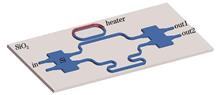
Silicon-Based Optical Flat-Top Filter with Ultrahigh Shape Factor
Shasha Liao, and Junxian Wu
ObjectiveFlat-top filters have been widely employed as channel selectors in wavelength division multiplexing systems due to their unique flat-top response characteristics, which can reduce the crosstalk among wavelengths and improve the rapidity and accuracy of channel optical detection. A large number of integrated schemes have been proposed and demonstrated in recent years, and most of them are based on silicon-on-insulator (SOI) platforms due to their capability for integration with electronics. However, these schemes have some disadvantages, with the schemes based on photonic crystal, waveguide grating, and cascaded microring resonators having a small fabrication tolerance. Meanwhile, schemes based on multistage cascaded Mach-Zehnder interferometer (MZI) have large footprints. Schemes based on microring resonator (MRR)-assisted MZI are proposed to achieve flat-top passband and small footprints, but in most previous schemes, an external phase shift of π or π/2 should be applied on the MRR or the long arm of MZI, which is difficult to achieve in practical fabrication due to the variations of effective refractive index and fabrication error. Additionally, some performance indexes such as the shape factor and ripple factor are not analyzed in these schemes. Therefore, we theoretically analyze and experimentally verify a flat-top filter with a high shape factor and low-complexity fabrication processing. Our scheme is based on the SOI platform and consists of a racetrack MRR (RMRR) and an asymmetric MZI. In our scheme, no external phase shift is needed. In addition, we analyze all key indicators of the filtering performance of a flat-top filter, especially the indicators that evaluate the filter shape including the shape factor and the ripple factor. Our scheme features a high shape factor, low-complexity fabrication processing, small size, light weight, and low power consumption. It can not only be widely adopted in high-speed optical network communication but also be designed as a part of the wavelength multiplexer by multi-stage cascading.MethodsOur flat-top filter consists of an asymmetric MZI coupler and an RMRR, with the MZI consisting of a pair of 2×2 multi-mode interferometers (MMIs). The input signal is divided into two light beams by the first MMI and transmits along the upper and lower arms of the MZI. The light beam in the upper arm is coupled into the RMMR to form an all-pass RMRR, and then the output light beam interferes with the light beam in the lower arm at the second MMI. A rectangular spectrum is generated ultimately. Due to the difficulty in realizing a phase shift of π or π/2 in practical fabrication, we ignore it and optimize the performance of our filter by adjusting other structural parameters such as the gap between RMRR and the short arm of MZI or the length of the coupling waveguide. A micro-heater is fabricated on the RMRR to investigate the effect of the phase shift introduced by RMRR on the performance of our flat-top filter.Results and DiscussionsThe bandwidth of 3 dB of our filter is 1.94 nm. The ripple factor and the sidelobe suppression ratio are about 2.40 dB and 7.45 dB respectively. The insertion loss and FSR are about 1.82 dB and 3.94 nm respectively (Fig. 6). It is irrational to measure the bandwidths of 10 dB and 15 dB under the sidelobe suppression ratio of less than 10 dB. However, the shape factor is a crucial performance indicator of the flat-top filter, and the sidelobe suppression ratio can be significantly improved by controlling the micro-heater fabricated on the coupling area of RMRR. Therefore, we still calculate the shape factor by the same method in the simulation. The widths of the passband are 2.02 nm and 2.06 nm when the passband power declines by 10 dB and 15 dB respectively. As a result, the shape factor is 0.96 (1.94/2.02) and 0.94 (1.94/2.06). Additionally, we also measure the output spectra while tuning the voltage applied on the RMRR. The central wavelength of our filter gradually experiences redshift, and the filtering performance periodically varies in the trend of degradation, improvement, and degradation, which is mainly because of the periodical variation of the phase shift introduced by RMRR with the increasing temperature. It indicates that tuning the phase shift introduced by RMRR can effectively control the output spectra of the filter.ConclusionsWe propose and demonstrate a flat-top filter with a high shape factor and low-complexity fabrication processing, and analyze all key indicators of the filtering performance of the flat-top filter, especially the indicators that evaluate the filter shape including the shape factor and the ripple factor. A filter with 3 dB bandwidths of 1.94 nm is realized. The corresponding shape factor 1 and shape factor 2 are 0.96 and 0.94 respectively. The ripple factor, the sidelobe suppression ratio, and the insertion loss are about 2.40 dB, 7.45 dB, and 1.82 dB respectively. Our scheme does not have energy loss throughout the transmission process as the spectra of the two output ports are complementary. Furthermore, we investigate the influence of the phase shift introduced by RMRR on the performance of our flat-top filter and verify that the performance of our filter will vary periodically by adjusting the voltage applied to the RMRR. Our scheme is characterized by a high shape factor, low-complexity fabrication processing, small size, light weight, and low power consumption. Additionally, it can not only be widely utilized in high-speed optical network communication but also be designed as a part of the wavelength multiplexer by multi-stage cascading. ObjectiveFlat-top filters have been widely employed as channel selectors in wavelength division multiplexing systems due to their unique flat-top response characteristics, which can reduce the crosstalk among wavelengths and improve the rapidity and accuracy of channel optical detection. A large number of integrated schemes have been proposed and demonstrated in recent years, and most of them are based on silicon-on-insulator (SOI) platforms due to their capability for integration with electronics. However, these schemes have some disadvantages, with the schemes based on photonic crystal, waveguide grating, and cascaded microring resonators having a small fabrication tolerance. Meanwhile, schemes based on multistage cascaded Mach-Zehnder interferometer (MZI) have large footprints. Schemes based on microring resonator (MRR)-assisted MZI are proposed to achieve flat-top passband and small footprints, but in most previous schemes, an external phase shift of π or π/2 should be applied on the MRR or the long arm of MZI, which is difficult to achieve in practical fabrication due to the variations of effective refractive index and fabrication error. Additionally, some performance indexes such as the shape factor and ripple factor are not analyzed in these schemes. Therefore, we theoretically analyze and experimentally verify a flat-top filter with a high shape factor and low-complexity fabrication processing. Our scheme is based on the SOI platform and consists of a racetrack MRR (RMRR) and an asymmetric MZI. In our scheme, no external phase shift is needed. In addition, we analyze all key indicators of the filtering performance of a flat-top filter, especially the indicators that evaluate the filter shape including the shape factor and the ripple factor. Our scheme features a high shape factor, low-complexity fabrication processing, small size, light weight, and low power consumption. It can not only be widely adopted in high-speed optical network communication but also be designed as a part of the wavelength multiplexer by multi-stage cascading.MethodsOur flat-top filter consists of an asymmetric MZI coupler and an RMRR, with the MZI consisting of a pair of 2×2 multi-mode interferometers (MMIs). The input signal is divided into two light beams by the first MMI and transmits along the upper and lower arms of the MZI. The light beam in the upper arm is coupled into the RMMR to form an all-pass RMRR, and then the output light beam interferes with the light beam in the lower arm at the second MMI. A rectangular spectrum is generated ultimately. Due to the difficulty in realizing a phase shift of π or π/2 in practical fabrication, we ignore it and optimize the performance of our filter by adjusting other structural parameters such as the gap between RMRR and the short arm of MZI or the length of the coupling waveguide. A micro-heater is fabricated on the RMRR to investigate the effect of the phase shift introduced by RMRR on the performance of our flat-top filter.Results and DiscussionsThe bandwidth of 3 dB of our filter is 1.94 nm. The ripple factor and the sidelobe suppression ratio are about 2.40 dB and 7.45 dB respectively. The insertion loss and FSR are about 1.82 dB and 3.94 nm respectively (Fig. 6). It is irrational to measure the bandwidths of 10 dB and 15 dB under the sidelobe suppression ratio of less than 10 dB. However, the shape factor is a crucial performance indicator of the flat-top filter, and the sidelobe suppression ratio can be significantly improved by controlling the micro-heater fabricated on the coupling area of RMRR. Therefore, we still calculate the shape factor by the same method in the simulation. The widths of the passband are 2.02 nm and 2.06 nm when the passband power declines by 10 dB and 15 dB respectively. As a result, the shape factor is 0.96 (1.94/2.02) and 0.94 (1.94/2.06). Additionally, we also measure the output spectra while tuning the voltage applied on the RMRR. The central wavelength of our filter gradually experiences redshift, and the filtering performance periodically varies in the trend of degradation, improvement, and degradation, which is mainly because of the periodical variation of the phase shift introduced by RMRR with the increasing temperature. It indicates that tuning the phase shift introduced by RMRR can effectively control the output spectra of the filter.ConclusionsWe propose and demonstrate a flat-top filter with a high shape factor and low-complexity fabrication processing, and analyze all key indicators of the filtering performance of the flat-top filter, especially the indicators that evaluate the filter shape including the shape factor and the ripple factor. A filter with 3 dB bandwidths of 1.94 nm is realized. The corresponding shape factor 1 and shape factor 2 are 0.96 and 0.94 respectively. The ripple factor, the sidelobe suppression ratio, and the insertion loss are about 2.40 dB, 7.45 dB, and 1.82 dB respectively. Our scheme does not have energy loss throughout the transmission process as the spectra of the two output ports are complementary. Furthermore, we investigate the influence of the phase shift introduced by RMRR on the performance of our flat-top filter and verify that the performance of our filter will vary periodically by adjusting the voltage applied to the RMRR. Our scheme is characterized by a high shape factor, low-complexity fabrication processing, small size, light weight, and low power consumption. Additionally, it can not only be widely utilized in high-speed optical network communication but also be designed as a part of the wavelength multiplexer by multi-stage cascading.
Acta Optica Sinica
- Publication Date: Apr. 10, 2024
- Vol. 44, Issue 7, 0723001 (2024)

Influence of Service Load and Structural Parameters on Optical Accuracy of Solar Tower Heliostat
Bin Li, Jian Yan, Wei Zhou, and Youduo Peng
ObjectiveSolar tower thermal power generation technology has the advantages of high light-electricity conversion efficiency and flexible energy storage, and it has become one of the most important ways to achieve the goal of “carbon peak and carbon neutrality”. The heliostat is the core device to realize solar energy pooling in the whole tower photovoltaic power plant. It can focus the solar energy within a certain range around the heat-absorbing tower, so as to complete the light-heat conversion in the heat-absorbing device with high quality. However, the heliostat is susceptible to structural deformation due to self-weight and wind load during service, and the distance between the heliostat and the heat-absorbing tower is relatively large. The small deformation of the reflecting mirror surface of the heliostat will lead to the reflected solar beam falling on the heat-absorbing device, which will directly lead to a decrease in the light-concentrating efficiency of the heliostat and a deterioration in the quality of the light-energy distribution of the heat-absorbing device. Therefore, it is important to investigate the service optical accuracy of the heliostat under self-weight and wind load, which can provide a basis for its lightweight and high-precision design and service performance guarantee.MethodsIn this study, we study a typical lightweight small-scale heliostat of 20 m2. First, we establishe the three-dimensional (3D) model and the finite element simulation model. Second, we adopte a universal optical-machine integration modeling method previously proposed by the team to consider the service deformation of solar concentrators and establishe an optical-mechanical integration analytical model of the heliostat. We also investigate the influence of the key structural parameters under the effect of self-weight and wind load on the optical accuracy of the heliostat in service. The structural parameters include the spacing d and the number N of the three rows of supporting bolts at the bottom of each plane mirror, the structural parameters of the frame supporting the mirrors, and the parameters of the beam cross-section. The conclusions of the study can provide an important basis for the design of lightweight high-precision heliostat and the maintenance of heliostat's performance in service.Results and DiscussionsWhen the wind pressure load on the mirror surface is equal, the self-load at a height angle of 90° has the most unfavorable influence on its optical accuracy. At N=7, the maximum deformation with height angle only increases from 2.07 mm to 2.63 mm, but Dx will significantly increase from 4.21 mrad to 5.35 mrad, and Dy will only increase from 1.36 mrad to 1.73 mrad (Fig. 3). Increasing the number of supporting bolts can reduce the concave deformation of the mirror surface between adjacent bolts in a single row, thereby reducing the slope error component Dy (Fig. 4). By comparing the distribution of mirror deformation and slope error, it can be clearly observed that the maximum slope error region does not occur in the maximum deformation region, which means that there is no non-linear positive correlation between mirror total slope error and mirror deformation (Fig. 5). The decrease in stiffness of the mirror itself is the main reason for the decrease in its optical accuracy, and a support rib plate structure should be added to the back of the mirror according to actual needs, so as to enhance its load-bearing stiffness (Fig. 6). Simply increasing the size of the cantilever secondary beam angle steel may not necessarily improve the optical accuracy of the mirror but rather result in material waste. To further improve optical accuracy, efforts should be made on the structural load-bearing stiffness of the mirror itself, such as adding a support plate on the back of the mirror (Figs. 7-8). The slope of the mirror total slope error variation curve at different height angles is basically the same, with only translation differences (Fig. 9).ConclusionsIf the frame structure is not deformed, the deformation and slope error of the mirror surface under the same wind pressure increase with the increase in the height angle of the heliostat mirror, and the slope error component Dx along the mirror surface in the transverse direction is significantly larger than Dy along its vertical direction; the increase in the number N of mirror back bolts does not have a significant effect on Dx, but it can significantly reduce Dy,and the improvement is no longer obvious when N≥11. There exists a reasonable value for the column spacing d to optimize the optical accuracy. In the example, the best parameters are d=950 mm and N=11, and the maximum deformation of the mirror surface is only 2.38 mm under 360 Pa wind pressure and self-weight. The errors of mirror slope Dx and Dy are only 5.31 mrad and 0.59 mrad. The structural deformations of the frame are only 0.72 mrad and 0.17 mrad to the Dx and Dy of the reflecting mirror surface. The structural stiffness of the frame is relatively affluent, and the stiffness of the reflecting mirror surface itself is the main reason for the degradation of its optical accuracy in service. The edge length a of the angle profiles in the rack between 30 mm and 50 mm has less effect on the service optical accuracy, while the effect of the thickness t is more significant. At t=4.0 mm, the service optical performance of a=30 mm and a=50 mm are comparable, and the former can reduce 1302 tons of steel in the case of the 50 MW solar tower power plant in Delingha, Qinghai. The preferred structural parameters are d=950 mm, N=11, H=380 mm, L=1225 mm, a=30 mm, and t=3.0 mm. Under different combinations of wind pressures (0-360 Pa) and height angles (0°, 45°, and 90°), the deformation of the structure and the error of the slope of the mirror surface increase linearly with the increase in the wind pressures, and the maximum deformation is in the range of 3.63-11.76 mm. While the slopes of the mirror total slope error change curves are basically the same for different height angles β, with only translational differences. When β=90°, the slope of the curve obtained by fitting the total mirror slope error with wind pressure is 0.0126, and the intercept is 1.439. Under the action of self-weight load only, the total slope error is in the range of 1.27-1.45 mrad for the height angles of 0°-90°. The distribution pattern of mirror deformation and its slope error is completely different. The relationship between mirror slope error and mirror deformation is not linear and proportional. In engineering practice, if the optimization design or evaluation of a heliostat structure is constrained by mirror deformation, satisfactory optical accuracy may not be obtained under a service load. Therefore, optical accuracy should be used to evaluate and guide the optimization design of the heliostat structure. ObjectiveSolar tower thermal power generation technology has the advantages of high light-electricity conversion efficiency and flexible energy storage, and it has become one of the most important ways to achieve the goal of “carbon peak and carbon neutrality”. The heliostat is the core device to realize solar energy pooling in the whole tower photovoltaic power plant. It can focus the solar energy within a certain range around the heat-absorbing tower, so as to complete the light-heat conversion in the heat-absorbing device with high quality. However, the heliostat is susceptible to structural deformation due to self-weight and wind load during service, and the distance between the heliostat and the heat-absorbing tower is relatively large. The small deformation of the reflecting mirror surface of the heliostat will lead to the reflected solar beam falling on the heat-absorbing device, which will directly lead to a decrease in the light-concentrating efficiency of the heliostat and a deterioration in the quality of the light-energy distribution of the heat-absorbing device. Therefore, it is important to investigate the service optical accuracy of the heliostat under self-weight and wind load, which can provide a basis for its lightweight and high-precision design and service performance guarantee.MethodsIn this study, we study a typical lightweight small-scale heliostat of 20 m2. First, we establishe the three-dimensional (3D) model and the finite element simulation model. Second, we adopte a universal optical-machine integration modeling method previously proposed by the team to consider the service deformation of solar concentrators and establishe an optical-mechanical integration analytical model of the heliostat. We also investigate the influence of the key structural parameters under the effect of self-weight and wind load on the optical accuracy of the heliostat in service. The structural parameters include the spacing d and the number N of the three rows of supporting bolts at the bottom of each plane mirror, the structural parameters of the frame supporting the mirrors, and the parameters of the beam cross-section. The conclusions of the study can provide an important basis for the design of lightweight high-precision heliostat and the maintenance of heliostat's performance in service.Results and DiscussionsWhen the wind pressure load on the mirror surface is equal, the self-load at a height angle of 90° has the most unfavorable influence on its optical accuracy. At N=7, the maximum deformation with height angle only increases from 2.07 mm to 2.63 mm, but Dx will significantly increase from 4.21 mrad to 5.35 mrad, and Dy will only increase from 1.36 mrad to 1.73 mrad (Fig. 3). Increasing the number of supporting bolts can reduce the concave deformation of the mirror surface between adjacent bolts in a single row, thereby reducing the slope error component Dy (Fig. 4). By comparing the distribution of mirror deformation and slope error, it can be clearly observed that the maximum slope error region does not occur in the maximum deformation region, which means that there is no non-linear positive correlation between mirror total slope error and mirror deformation (Fig. 5). The decrease in stiffness of the mirror itself is the main reason for the decrease in its optical accuracy, and a support rib plate structure should be added to the back of the mirror according to actual needs, so as to enhance its load-bearing stiffness (Fig. 6). Simply increasing the size of the cantilever secondary beam angle steel may not necessarily improve the optical accuracy of the mirror but rather result in material waste. To further improve optical accuracy, efforts should be made on the structural load-bearing stiffness of the mirror itself, such as adding a support plate on the back of the mirror (Figs. 7-8). The slope of the mirror total slope error variation curve at different height angles is basically the same, with only translation differences (Fig. 9).ConclusionsIf the frame structure is not deformed, the deformation and slope error of the mirror surface under the same wind pressure increase with the increase in the height angle of the heliostat mirror, and the slope error component Dx along the mirror surface in the transverse direction is significantly larger than Dy along its vertical direction; the increase in the number N of mirror back bolts does not have a significant effect on Dx, but it can significantly reduce Dy,and the improvement is no longer obvious when N≥11. There exists a reasonable value for the column spacing d to optimize the optical accuracy. In the example, the best parameters are d=950 mm and N=11, and the maximum deformation of the mirror surface is only 2.38 mm under 360 Pa wind pressure and self-weight. The errors of mirror slope Dx and Dy are only 5.31 mrad and 0.59 mrad. The structural deformations of the frame are only 0.72 mrad and 0.17 mrad to the Dx and Dy of the reflecting mirror surface. The structural stiffness of the frame is relatively affluent, and the stiffness of the reflecting mirror surface itself is the main reason for the degradation of its optical accuracy in service. The edge length a of the angle profiles in the rack between 30 mm and 50 mm has less effect on the service optical accuracy, while the effect of the thickness t is more significant. At t=4.0 mm, the service optical performance of a=30 mm and a=50 mm are comparable, and the former can reduce 1302 tons of steel in the case of the 50 MW solar tower power plant in Delingha, Qinghai. The preferred structural parameters are d=950 mm, N=11, H=380 mm, L=1225 mm, a=30 mm, and t=3.0 mm. Under different combinations of wind pressures (0-360 Pa) and height angles (0°, 45°, and 90°), the deformation of the structure and the error of the slope of the mirror surface increase linearly with the increase in the wind pressures, and the maximum deformation is in the range of 3.63-11.76 mm. While the slopes of the mirror total slope error change curves are basically the same for different height angles β, with only translational differences. When β=90°, the slope of the curve obtained by fitting the total mirror slope error with wind pressure is 0.0126, and the intercept is 1.439. Under the action of self-weight load only, the total slope error is in the range of 1.27-1.45 mrad for the height angles of 0°-90°. The distribution pattern of mirror deformation and its slope error is completely different. The relationship between mirror slope error and mirror deformation is not linear and proportional. In engineering practice, if the optimization design or evaluation of a heliostat structure is constrained by mirror deformation, satisfactory optical accuracy may not be obtained under a service load. Therefore, optical accuracy should be used to evaluate and guide the optimization design of the heliostat structure.
Acta Optica Sinica
- Publication Date: Mar. 25, 2024
- Vol. 44, Issue 6, 0623001 (2024)
Design of Tunable Four-Broadband Terahertz Absorber
Ting Zhang, Taiming Guo, Junya Yan, and Yanan Pei
ObjectiveSince the first metamaterial perfect absorber was proposed by Landy et al., it has been widely developed due to its potential applications in the fields of microwave radiation measurement, biosensors, thermal emitters, and imaging. Many existing absorbers face the issue of narrow bandwidths, which fail to satisfy the demands of some optoelectronic devices. To solve this problem, it is common to construct different patterns in the same layer or stack multilayer structures with different geometrical dimensions. However, these structures are often complex, and the absorption rate cannot be actively adjusted. Therefore, phase change materials have been introduced to regulate the absorption rate of absorbents, and vanadium dioxide is one of them. There are many absorbers designed with VO2, but the absorption bandwidth and band number need to be further increased. Therefore, combining the characteristics of multi-band, wideband, and tunable absorption remains a meaningful endeavor.MethodsTo effectively study the performance of the absorber, the proposed structure is analyzed by using the microwave simulation software CST Microwave Studio 2020. The metamaterial absorber in this study consists of three layers: the top layer VO2, the middle layer SiO2, and the bottom layer Au. When the conductivity is adjusted from 200 S/m to 2×10⁵ S/m, VO2 will change from an insulator to metal, which can be simulated by input conductivity parameters through the Drude model in CST software. The absorber's absorption can be obtained through one minus the reflection and transmission. Since the penetration depth of the incident wave is smaller than the Au thickness, thus the transmittance is zero. Perfect absorption can be achieved when the reflection is also zero. Material selection and structural design are used to achieve impedance matching, ensuring zero reflection and ultimately realizing perfect absorption of multiple broadbands.Results and DiscussionsThe simulation results show that there are four absorption bands with more than 90% of absorptivity in the range of 0-10 THz, covering bandwidths of 0.87, 0.58, 0.61, and 0.45 THz, respectively. With variations in the conductivity of VO2, the absorptivity dynamically adjusts between 7.7% and 99.9% (Fig. 2). The analysis finds that with the change of dielectric constant of vanadium dioxide, the resonant frequency remains almost constant, while the absorption rate changes significantly. The Fabry-Perot resonance theory and impedance matching theory are introduced to explain the effects of the dielectric layer and the VO2 layer on the absorption (Figs. 3-5). The physical sources of multiple perfect absorption peaks are analyzed through the electric field distribution (Fig. 6). Additionally, changes in absorptivity with different incident angles and polarization angles are analyzed (Fig. 7), which shows that the absorber has the characteristics of polarization insensitivity and wide-angle absorption.ConclusionsWe describe a terahertz absorber with four absorption bands, dynamically adjustable absorptivity, and a simple structure. Simulation results indicate that within the range of 0-10 THz, there are four absorption bands with more than 90% absorptivity, and their respective bandwidths are 0.87, 0.58, 0.61, and 0.45 THz. The absorptivity can be dynamically adjusted between 7.7% and 99.9% by varying the conductivity of vanadium dioxide. The physical mechanism of the absorber is explained using impedance matching theory and Fabry-Perot resonance theory. Through the analysis of the electric field distribution, it is found that the first broadband absorption is mainly caused by the local absorption of VO2, while the second, third, and fourth broadband absorptions result from the resonance absorption of multiple electric dipoles on the surface of VO2, coupled with the coupling effects between the dielectric layer and VO2 and the metal layer. Additionally, it has the features of wide-angle absorption and polarization insensitivity. This absorber has potential applications in micro-radiometers, biosensors, stealth technology, and other fields. ObjectiveSince the first metamaterial perfect absorber was proposed by Landy et al., it has been widely developed due to its potential applications in the fields of microwave radiation measurement, biosensors, thermal emitters, and imaging. Many existing absorbers face the issue of narrow bandwidths, which fail to satisfy the demands of some optoelectronic devices. To solve this problem, it is common to construct different patterns in the same layer or stack multilayer structures with different geometrical dimensions. However, these structures are often complex, and the absorption rate cannot be actively adjusted. Therefore, phase change materials have been introduced to regulate the absorption rate of absorbents, and vanadium dioxide is one of them. There are many absorbers designed with VO2, but the absorption bandwidth and band number need to be further increased. Therefore, combining the characteristics of multi-band, wideband, and tunable absorption remains a meaningful endeavor.MethodsTo effectively study the performance of the absorber, the proposed structure is analyzed by using the microwave simulation software CST Microwave Studio 2020. The metamaterial absorber in this study consists of three layers: the top layer VO2, the middle layer SiO2, and the bottom layer Au. When the conductivity is adjusted from 200 S/m to 2×10⁵ S/m, VO2 will change from an insulator to metal, which can be simulated by input conductivity parameters through the Drude model in CST software. The absorber's absorption can be obtained through one minus the reflection and transmission. Since the penetration depth of the incident wave is smaller than the Au thickness, thus the transmittance is zero. Perfect absorption can be achieved when the reflection is also zero. Material selection and structural design are used to achieve impedance matching, ensuring zero reflection and ultimately realizing perfect absorption of multiple broadbands.Results and DiscussionsThe simulation results show that there are four absorption bands with more than 90% of absorptivity in the range of 0-10 THz, covering bandwidths of 0.87, 0.58, 0.61, and 0.45 THz, respectively. With variations in the conductivity of VO2, the absorptivity dynamically adjusts between 7.7% and 99.9% (Fig. 2). The analysis finds that with the change of dielectric constant of vanadium dioxide, the resonant frequency remains almost constant, while the absorption rate changes significantly. The Fabry-Perot resonance theory and impedance matching theory are introduced to explain the effects of the dielectric layer and the VO2 layer on the absorption (Figs. 3-5). The physical sources of multiple perfect absorption peaks are analyzed through the electric field distribution (Fig. 6). Additionally, changes in absorptivity with different incident angles and polarization angles are analyzed (Fig. 7), which shows that the absorber has the characteristics of polarization insensitivity and wide-angle absorption.ConclusionsWe describe a terahertz absorber with four absorption bands, dynamically adjustable absorptivity, and a simple structure. Simulation results indicate that within the range of 0-10 THz, there are four absorption bands with more than 90% absorptivity, and their respective bandwidths are 0.87, 0.58, 0.61, and 0.45 THz. The absorptivity can be dynamically adjusted between 7.7% and 99.9% by varying the conductivity of vanadium dioxide. The physical mechanism of the absorber is explained using impedance matching theory and Fabry-Perot resonance theory. Through the analysis of the electric field distribution, it is found that the first broadband absorption is mainly caused by the local absorption of VO2, while the second, third, and fourth broadband absorptions result from the resonance absorption of multiple electric dipoles on the surface of VO2, coupled with the coupling effects between the dielectric layer and VO2 and the metal layer. Additionally, it has the features of wide-angle absorption and polarization insensitivity. This absorber has potential applications in micro-radiometers, biosensors, stealth technology, and other fields.
Acta Optica Sinica
- Publication Date: Mar. 10, 2024
- Vol. 44, Issue 5, 0523002 (2024)
On-Chip Mode Splitter with Mode Maintenance Function
Shasha Liao, Wuhao Zhang, Shuai Zhao, Xincheng Zhao, and Liang Tang
ObjectiveThe mode splitter is employed in mode division multiplexing systems to separate and guide different modes in a bus waveguide. Traditional mode splitter methods are based on mode conversion processes, where the input higher-order modes are converted into the fundamental mode to separate them from the bus waveguide. This method is suitable for most mode division multiplexing systems, but in scenarios such as signal routing or signal selection, when different modes are separated, they are often switched or selected using multi-mode switches. If the mode splitter output is all in the fundamental mode, additional components should be added after the mode splitter to convert the separated fundamental mode back to higher-order modes before inputting them into multi-mode switches, which undoubtedly increases the system complexity. In the case of optical isolation, it is often necessary to remove the higher-order modes and just transmit the fundamental mode. If the mode splitter output is all in the fundamental mode, it cannot meet the requirements of practical applications. Therefore, if the original modes can be preserved with mode separation achieved, this will greatly simplify the system structure and reduce the system size.MethodsThe multi-mode interference (MMI) coupler is a basic silicon-based device, that features a compact structure, low loss, and easy fabrication. However, traditional MMI-based mode splitters are difficult to extend the mode separation function to higher-order modes due to the highly symmetric structure and mode self-imaging principle. This scheme is based on the silicon-on-insulator (SOI) platform. According to the modal analysis method, it is derived that the refractive index distribution in the multi-mode region can not only change the imaging position and shorten the self-imaging length but also separate different input modes. Thermal tuning is achieved by fabricating heaters on top of the waveguide, and the waveguide material refractive index changes with the temperature at a rate of 1.84×10⁻⁴ K-1 due to the thermo-optic effect. Therefore, by adding micro heaters to the multi-mode region of the MMI, designing the positions of the heaters, and accurately controlling the heating temperature, the separation of three modes, TE0, TE1, and TE2 can be achieved.Results and DiscussionsThe designed structure is a 1×3 MMI, with the input port of the MMI located at the upper left of the multi-mode region, and four heaters are uniformly distributed in the multi-mode region. The optimized size parameters are w=w3=1.9 μm, w1=0.9 μm, w2=0.6 μm, wtaper=wtaper1=wtaper3=4.4 μm, wtaper2=6 μm, wm=15 μm, and lm=227 μm (Fig. 6). The heating temperatures of the four heaters for the TE0 mode are 32 ℃, 26.14 ℃, 0 ℃, and 43.42 ℃ respectively, temperatures for the TE1 mode are 7.61 ℃, 0 ℃, 50 ℃, and 17.89 ℃, and those for the TE2 mode are 50 ℃, 50 ℃, 4.89 ℃, and 50 ℃. Under the wavelength of 1550 nm, the insertion losses are 1.03 dB, 1.04 dB, and 1.06 dB for the three modes, the crosstalks are -15.38 dB, -17.5 dB, and -20.4 dB respectively, and all have a 3 dB bandwidth greater than 97 nm (Fig. 8). It is proven that compared with traditional mode splitters, the proposed scheme has a larger number of separated modes, smaller insertion losses, and smaller mode crosstalks. The most outstanding feature is that it preserves the original modes during mode separation, which makes it have a wider range of applications in mode division multiplexing systems. Additionally, by increasing the number of micro heaters and output waveguides, the proposed scheme can achieve the separation of higher-order and more modes.ConclusionsAn MMI-based on-chip mode splitter scheme is proposed to separate the first three TE modes (TE0, TE1, and TE2) and preserve the modes. When the wavelength is 1550 nm, the insertion losses are 1.03 dB, 1.04 dB, and 1.06 dB, and the crosstalks are -15.38 dB, -17.5 dB, and -20.4 dB, with a 3 dB bandwidth greater than 97 nm. Meanwhile, when the temperature deviation is within 2 ℃, the insertion loss of each mode is less than 1.45 dB, and the crosstalkis less than -13.22 dB. Compared with traditional mode splitters based on mode demultiplexers, the proposed scheme can achieve separation without converting high-order modes into fundamental modes, which can greatly reduce system complexity in scenarios such as signal routing or signal selection. As more heaters are added, the proposed scheme can be expanded to separate higher-order modes. At the same time, this mode splitter also has high integration and low process difficulty and can be widely employed in optical communication systems. ObjectiveThe mode splitter is employed in mode division multiplexing systems to separate and guide different modes in a bus waveguide. Traditional mode splitter methods are based on mode conversion processes, where the input higher-order modes are converted into the fundamental mode to separate them from the bus waveguide. This method is suitable for most mode division multiplexing systems, but in scenarios such as signal routing or signal selection, when different modes are separated, they are often switched or selected using multi-mode switches. If the mode splitter output is all in the fundamental mode, additional components should be added after the mode splitter to convert the separated fundamental mode back to higher-order modes before inputting them into multi-mode switches, which undoubtedly increases the system complexity. In the case of optical isolation, it is often necessary to remove the higher-order modes and just transmit the fundamental mode. If the mode splitter output is all in the fundamental mode, it cannot meet the requirements of practical applications. Therefore, if the original modes can be preserved with mode separation achieved, this will greatly simplify the system structure and reduce the system size.MethodsThe multi-mode interference (MMI) coupler is a basic silicon-based device, that features a compact structure, low loss, and easy fabrication. However, traditional MMI-based mode splitters are difficult to extend the mode separation function to higher-order modes due to the highly symmetric structure and mode self-imaging principle. This scheme is based on the silicon-on-insulator (SOI) platform. According to the modal analysis method, it is derived that the refractive index distribution in the multi-mode region can not only change the imaging position and shorten the self-imaging length but also separate different input modes. Thermal tuning is achieved by fabricating heaters on top of the waveguide, and the waveguide material refractive index changes with the temperature at a rate of 1.84×10⁻⁴ K-1 due to the thermo-optic effect. Therefore, by adding micro heaters to the multi-mode region of the MMI, designing the positions of the heaters, and accurately controlling the heating temperature, the separation of three modes, TE0, TE1, and TE2 can be achieved.Results and DiscussionsThe designed structure is a 1×3 MMI, with the input port of the MMI located at the upper left of the multi-mode region, and four heaters are uniformly distributed in the multi-mode region. The optimized size parameters are w=w3=1.9 μm, w1=0.9 μm, w2=0.6 μm, wtaper=wtaper1=wtaper3=4.4 μm, wtaper2=6 μm, wm=15 μm, and lm=227 μm (Fig. 6). The heating temperatures of the four heaters for the TE0 mode are 32 ℃, 26.14 ℃, 0 ℃, and 43.42 ℃ respectively, temperatures for the TE1 mode are 7.61 ℃, 0 ℃, 50 ℃, and 17.89 ℃, and those for the TE2 mode are 50 ℃, 50 ℃, 4.89 ℃, and 50 ℃. Under the wavelength of 1550 nm, the insertion losses are 1.03 dB, 1.04 dB, and 1.06 dB for the three modes, the crosstalks are -15.38 dB, -17.5 dB, and -20.4 dB respectively, and all have a 3 dB bandwidth greater than 97 nm (Fig. 8). It is proven that compared with traditional mode splitters, the proposed scheme has a larger number of separated modes, smaller insertion losses, and smaller mode crosstalks. The most outstanding feature is that it preserves the original modes during mode separation, which makes it have a wider range of applications in mode division multiplexing systems. Additionally, by increasing the number of micro heaters and output waveguides, the proposed scheme can achieve the separation of higher-order and more modes.ConclusionsAn MMI-based on-chip mode splitter scheme is proposed to separate the first three TE modes (TE0, TE1, and TE2) and preserve the modes. When the wavelength is 1550 nm, the insertion losses are 1.03 dB, 1.04 dB, and 1.06 dB, and the crosstalks are -15.38 dB, -17.5 dB, and -20.4 dB, with a 3 dB bandwidth greater than 97 nm. Meanwhile, when the temperature deviation is within 2 ℃, the insertion loss of each mode is less than 1.45 dB, and the crosstalkis less than -13.22 dB. Compared with traditional mode splitters based on mode demultiplexers, the proposed scheme can achieve separation without converting high-order modes into fundamental modes, which can greatly reduce system complexity in scenarios such as signal routing or signal selection. As more heaters are added, the proposed scheme can be expanded to separate higher-order modes. At the same time, this mode splitter also has high integration and low process difficulty and can be widely employed in optical communication systems.
Acta Optica Sinica
- Publication Date: Mar. 10, 2024
- Vol. 44, Issue 5, 0523001 (2024)
Tunable Terahertz Coding Metasurface with Switchable Frequency Bands
Jingli Wang, Zhixiong Yang, Liang Yin, Xianchao Dong, Hongdan Wan, Heming Chen, and Kai Zhong
ObjectiveTerahertz waves are electromagnetic waves between microwave and infrared wave with the frequency of 0.1-10 THz and feature strong penetration, large information capacity, high security, and strong maneuverability. Additionally, they have extensive applications in remote communication, security imaging, radar detection, and other fields. With the increasing number of application scenarios, there is an urgent need for functional devices that can regulate terahertz waves in multiple frequency bands. As an important device to regulate terahertz waves, the coding metasurface is characterized by the phase response properties of the coding metasurface units by binary digital code and arranges the coding metasurface units according to the coding sequence to achieve flexible wave regulation. Meanwhile, it can generate various beam forms such as vortex waves, deflection waves, and focused waves. However, once a traditional coding metasurface is designed, it can only generate a beam form at a single frequency point, limiting the working frequency range of the coding metasurface. As a kind of phase change material, vanadium dioxide (VO2) can change its temperature by electricity, heat, and light to achieve phase change function, and is widely applied to metasurface design. Some studies implement the function of generating different beam forms by different coding sequences, but the working frequency band is single and cannot be switched. Another study adopts the PB phase principle combined with VO2 to design a frequency switchable coding metasurface, which achieves vortex wave generation at different frequency points. However, it only yields good results at three frequency points, limiting the working frequency range. Therefore, it is significant to broaden the working frequency range of the coding metasurface and achieve frequency band switching.MethodsFirst, a new type of coding metasurface unit is designed by combining the PB phase principle with the VO2 phase transition characteristics. By rotating the unit at a certain angle and changing the phase transition state of VO2, the reflection amplitude and phase in different working frequency ranges are studied. The conditions are as follows. When VO2 is in an insulated state and a metallic state, it works in different frequency bands respectively and meets the conditions of 3-bit coding metasurface unit in the corresponding frequency band. Then, by taking the terahertz metasurface which can generate high-capacity vortex waves and high RCS reduced scattering waves as an example, a coding sequence is designed. Finally, the wave forms generated by the coding metasurface are simulated at different frequencies to study whether the beam form corresponding to the coding sequence can be generated. By changing the phase transition state of VO2, switching of the operating frequency band can be achieved.Results and DiscussionsBy rotating the designed metasurface units (Fig. 1) counterclockwise in a step of 22.5° from 0° to 157.5°, eight metasurface units can be obtained (Table 1). The unit analysis based on the two phase transition states of VO2 shows that when VO2 is in an insulated state, the unit maintains a large reflection amplitude between 1.17 THz and 1.37 THz, and the phase difference of the eight units strictly meets a 45° phase difference. When VO2 is in a metallic state, it maintains a large amplitude and a phase difference of 45° in sequence at 0.87-0.92 THz and 1.4-1.6 THz. Therefore, at all three frequency bands, the metasurface unit meets the design conditions for a 3-bit coding metasurface unit. The coding metasurface units are arranged according to a certain coding sequence, the coding metasurface formed by them can flexibly regulate terahertz waves, and its mechanism of regulating terahertz waves is similar to traditional phased array antenna theory (Formula 1). Therefore, the designed coding metasurface units are arranged according to the coding sequence that generates vortex waves with topological charge number 1 (Fig. 4) and scattered waves that can reduce RCS (Fig. 6). The results show that VO2 can generate the same beams with the same coding sequence at different operating frequency bands under different phase transition states, and the operating frequency band can change with the phase transition state of VO2.ConclusionsBased on the PB phase principle and phase change material VO2, we design the 3-bit coding metasurface units. A variety of coding metasurfaces are formed by different coding sequence arrangements, which can regulate terahertz waves to generate beam forms corresponding to the coding sequences. Under an insulated state, VO2 works in a single frequency band of 1.17-1.37 THz, and it works in dual bands of 0.87-0.92 THz and 1.4-1.6 THz in a metallic state. The designed VO2 based on coding metasurface can switch the frequency bands without changing the wave forms, and provide important ideas for frequency modulation of terahertz waves. ObjectiveTerahertz waves are electromagnetic waves between microwave and infrared wave with the frequency of 0.1-10 THz and feature strong penetration, large information capacity, high security, and strong maneuverability. Additionally, they have extensive applications in remote communication, security imaging, radar detection, and other fields. With the increasing number of application scenarios, there is an urgent need for functional devices that can regulate terahertz waves in multiple frequency bands. As an important device to regulate terahertz waves, the coding metasurface is characterized by the phase response properties of the coding metasurface units by binary digital code and arranges the coding metasurface units according to the coding sequence to achieve flexible wave regulation. Meanwhile, it can generate various beam forms such as vortex waves, deflection waves, and focused waves. However, once a traditional coding metasurface is designed, it can only generate a beam form at a single frequency point, limiting the working frequency range of the coding metasurface. As a kind of phase change material, vanadium dioxide (VO2) can change its temperature by electricity, heat, and light to achieve phase change function, and is widely applied to metasurface design. Some studies implement the function of generating different beam forms by different coding sequences, but the working frequency band is single and cannot be switched. Another study adopts the PB phase principle combined with VO2 to design a frequency switchable coding metasurface, which achieves vortex wave generation at different frequency points. However, it only yields good results at three frequency points, limiting the working frequency range. Therefore, it is significant to broaden the working frequency range of the coding metasurface and achieve frequency band switching.MethodsFirst, a new type of coding metasurface unit is designed by combining the PB phase principle with the VO2 phase transition characteristics. By rotating the unit at a certain angle and changing the phase transition state of VO2, the reflection amplitude and phase in different working frequency ranges are studied. The conditions are as follows. When VO2 is in an insulated state and a metallic state, it works in different frequency bands respectively and meets the conditions of 3-bit coding metasurface unit in the corresponding frequency band. Then, by taking the terahertz metasurface which can generate high-capacity vortex waves and high RCS reduced scattering waves as an example, a coding sequence is designed. Finally, the wave forms generated by the coding metasurface are simulated at different frequencies to study whether the beam form corresponding to the coding sequence can be generated. By changing the phase transition state of VO2, switching of the operating frequency band can be achieved.Results and DiscussionsBy rotating the designed metasurface units (Fig. 1) counterclockwise in a step of 22.5° from 0° to 157.5°, eight metasurface units can be obtained (Table 1). The unit analysis based on the two phase transition states of VO2 shows that when VO2 is in an insulated state, the unit maintains a large reflection amplitude between 1.17 THz and 1.37 THz, and the phase difference of the eight units strictly meets a 45° phase difference. When VO2 is in a metallic state, it maintains a large amplitude and a phase difference of 45° in sequence at 0.87-0.92 THz and 1.4-1.6 THz. Therefore, at all three frequency bands, the metasurface unit meets the design conditions for a 3-bit coding metasurface unit. The coding metasurface units are arranged according to a certain coding sequence, the coding metasurface formed by them can flexibly regulate terahertz waves, and its mechanism of regulating terahertz waves is similar to traditional phased array antenna theory (Formula 1). Therefore, the designed coding metasurface units are arranged according to the coding sequence that generates vortex waves with topological charge number 1 (Fig. 4) and scattered waves that can reduce RCS (Fig. 6). The results show that VO2 can generate the same beams with the same coding sequence at different operating frequency bands under different phase transition states, and the operating frequency band can change with the phase transition state of VO2.ConclusionsBased on the PB phase principle and phase change material VO2, we design the 3-bit coding metasurface units. A variety of coding metasurfaces are formed by different coding sequence arrangements, which can regulate terahertz waves to generate beam forms corresponding to the coding sequences. Under an insulated state, VO2 works in a single frequency band of 1.17-1.37 THz, and it works in dual bands of 0.87-0.92 THz and 1.4-1.6 THz in a metallic state. The designed VO2 based on coding metasurface can switch the frequency bands without changing the wave forms, and provide important ideas for frequency modulation of terahertz waves.
Acta Optica Sinica
- Publication Date: Feb. 10, 2024
- Vol. 44, Issue 3, 0323002 (2024)
Omnidirectional Dual-Function Terahertz Metasurface Device
Lina Zhang, and Jiusheng Li
ObjectiveMetasurface effective and flexible manipulation of electromagnetic waves in sub-wavelength size has attracted widespread attention. Many metasurface-based devices have been reported in recent years, such as anomalous reflectors/refractometers, vortex beam generators, and polarization converters. However, most reported metasurfaces can only manipulate transmitted or reflected electromagnetic waves. Due to the limitations of half-space manipulation of terahertz waves, it is necessary to design a full-space metasurface, which can realize the manipulation of terahertz waves with reflected and transmitted modes. However, the reported full-space metasurfaces can only manipulate one of the polarized waves for circularly polarized and linearly polarized waves. Therefore, it is very urgent to design a metasurface that can simultaneously reflect and transmit terahertz waves of both circularly polarized and linearly polarized waves.MethodsIn this paper, we propose an omnidirectional bifunctional terahertz metasurface to generate the modulation of radiometric polarization and reflect circularly polarized waves. The unit cell has nine layers, which are elliptical metal pattern, polyimide, metal grating, polyimide, rectangular metal strip structure, polyimide, metal grating, polyimide, and elliptical metal pattern. When a circularly polarized terahertz wave is incident in the metasurface, it can produce reflected vortex beam splitting, deflection vortices, and superimposed vortices. When the y(x) linearly polarized wave is incident along the ±z direction, the designed metasurface produces the x(y) linearly polarized wave transmission and transformation. This terahertz metasurface device offers great flexibility in terahertz wave regulation.Results and DiscussionsWhen the circularly polarized terahertz wave is incident, the metasurface structure generates vortex beams with topological charges of l=±1 and ±2 at frequencies of 1.4 THz and 1.5 THz, four offset vortex beams with l=-1 and +2 at 1.3 THz, andsuperposition vortex beams with l=-1 and +2 at 1.5 THz. When the linearly polarized terahertz wave is incident along the ±z direction, the designed metasurface realizes the polarization conversion function of the transmitted wave at the frequency of 0.72 THz, and the polarization conversion rate is greater than 95%. This metasurface provides an innovative idea for the design of bidirectional multifunctional terahertz wave control devices.ConclusionsIn this paper, an omnidirectional bifunctional terahertz metasurface device is proposed, and the metasurface element structure is composed of the top elliptical metal pattern, polyimide, metal grating, polyimide, rectangular metal strip, polyimide, metal grating, polyimide, and elliptical metal pattern from top to bottom. When circularly polarized terahertz waves are incident to the metasurface, vortex beams with topological charges of l=±1 and ±2 are generated at frequencies 1.4 THz and 1.5 THz. Four vortex beams with l=-1 and one deflected vortex beam with l=+2 are generated at 1.3 THz, and superposition vortex beams with l=-1 and +2 are generated at 1.5 THz. When the y(x) polarized wave is incident to the metasurface from the -z(+z) direction, a transmission mode x(y) polarization wave is generated at 0.72 THz. The omnidirectional bifunctional terahertz metasurface proposed in this paper provides a new idea for manipulating terahertz waves with multi-polarized and bidirectional terahertz waves. ObjectiveMetasurface effective and flexible manipulation of electromagnetic waves in sub-wavelength size has attracted widespread attention. Many metasurface-based devices have been reported in recent years, such as anomalous reflectors/refractometers, vortex beam generators, and polarization converters. However, most reported metasurfaces can only manipulate transmitted or reflected electromagnetic waves. Due to the limitations of half-space manipulation of terahertz waves, it is necessary to design a full-space metasurface, which can realize the manipulation of terahertz waves with reflected and transmitted modes. However, the reported full-space metasurfaces can only manipulate one of the polarized waves for circularly polarized and linearly polarized waves. Therefore, it is very urgent to design a metasurface that can simultaneously reflect and transmit terahertz waves of both circularly polarized and linearly polarized waves.MethodsIn this paper, we propose an omnidirectional bifunctional terahertz metasurface to generate the modulation of radiometric polarization and reflect circularly polarized waves. The unit cell has nine layers, which are elliptical metal pattern, polyimide, metal grating, polyimide, rectangular metal strip structure, polyimide, metal grating, polyimide, and elliptical metal pattern. When a circularly polarized terahertz wave is incident in the metasurface, it can produce reflected vortex beam splitting, deflection vortices, and superimposed vortices. When the y(x) linearly polarized wave is incident along the ±z direction, the designed metasurface produces the x(y) linearly polarized wave transmission and transformation. This terahertz metasurface device offers great flexibility in terahertz wave regulation.Results and DiscussionsWhen the circularly polarized terahertz wave is incident, the metasurface structure generates vortex beams with topological charges of l=±1 and ±2 at frequencies of 1.4 THz and 1.5 THz, four offset vortex beams with l=-1 and +2 at 1.3 THz, andsuperposition vortex beams with l=-1 and +2 at 1.5 THz. When the linearly polarized terahertz wave is incident along the ±z direction, the designed metasurface realizes the polarization conversion function of the transmitted wave at the frequency of 0.72 THz, and the polarization conversion rate is greater than 95%. This metasurface provides an innovative idea for the design of bidirectional multifunctional terahertz wave control devices.ConclusionsIn this paper, an omnidirectional bifunctional terahertz metasurface device is proposed, and the metasurface element structure is composed of the top elliptical metal pattern, polyimide, metal grating, polyimide, rectangular metal strip, polyimide, metal grating, polyimide, and elliptical metal pattern from top to bottom. When circularly polarized terahertz waves are incident to the metasurface, vortex beams with topological charges of l=±1 and ±2 are generated at frequencies 1.4 THz and 1.5 THz. Four vortex beams with l=-1 and one deflected vortex beam with l=+2 are generated at 1.3 THz, and superposition vortex beams with l=-1 and +2 are generated at 1.5 THz. When the y(x) polarized wave is incident to the metasurface from the -z(+z) direction, a transmission mode x(y) polarization wave is generated at 0.72 THz. The omnidirectional bifunctional terahertz metasurface proposed in this paper provides a new idea for manipulating terahertz waves with multi-polarized and bidirectional terahertz waves.
Acta Optica Sinica
- Publication Date: Feb. 10, 2024
- Vol. 44, Issue 3, 0323001 (2024)
Topics
© Copyright 2018-2021 | Chinese Laser Press. All Rights Reserved 沪ICP备15018463号-20